The circuit below shows a simple but effective way to power activate a (DC) device by pressing a button. The device can be completly switched of electronically (e.g. by a microcontroller). (Switch SW2 if only shown to demonstrate the operation principle of the circuit.)
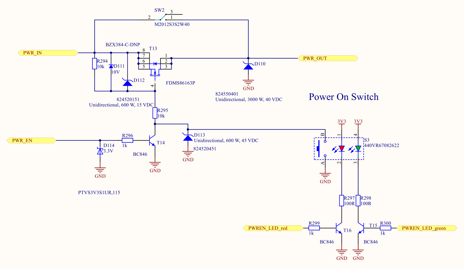
Depending on the selected P-channel MOSFET T13 the circuit can handle voltages bigger of more than 60V and currents of several tens of amperes.
The same functionality could be achieved by a relay at the expense of volume (relay is much bigger) and power consumption (~100mW or more). Especially in a battery powered portable application, there is no way for a relay.
Circuit description
Power enters the schematic at the PWR_IN port (top left). In OFF-state the MOSFET handling the power (T13) is blocking current from its source to drain. Please note the body diode of the MOSFET is in reverse to the current flowing from PWR_IN to PWR_OUT when MOSFET is conducting. In the OFF-State the gate of T13 is pulled to the PWR_IN voltage level via pull-up resistor R294 thus keeping the MOSFET not conducting. The value of R294 is selected to keep safe operation at minimal losses when the gate is pulled low.
To activate the device the user will press the activation switch S3 which closes the contacts A-B and pulling the gate of T13 to GND. As soon as the gate-source voltage at the gate of the MOSFET drops below Vgs_th (threshold voltage see the datasheet of your preferred MOSFET) T13 will start conducting. As current flows from PWR_IN to PWR_OUT a microcontroller connected to PWR_EN can boot and then control the bipolar NPN transistor T14 which will pull the gate towards GND, too. As the microcontroller starts to work it immediately needs to output high level (3,3V or 5V) to T14. After this, the button can be released by the user. The sequence to power a microcontroller should take less than 1ms.
Remaining components are mostly protecting the MOSFET and the microcontroller pin. One big problem with this kind of circuit is the limited gate-source voltage of most modern MOSFET. The majority of them will take permanent damage if the gate-source voltage (Vgs) is bigger than (-)20V. If you want to use this circuit in a 24V or even 48V environment Vgs needs to be limited. This is done by the zener diode D111. Across D111 there is a constant voltage drop of the zener voltage (chosen to be 10V here). At this voltage, Vgs is big enough to keep T13 fully conducting. D111 forms a voltage divider in conjunction with R295. TVS diodes D110 and D112 further protect T13 against voltage transients and act as a basic over voltage circuit (requiring a fuse elsewhere before this circuit!). D113 is used to protect the bipolar NPN transistor T14 in the case of an overvoltage event. R296 acts as current limiting resistor into T14 in order to limit the current out of the microcontroller pin. For T14 any NPN (e.g. BC817, BC547, BC548, …) should be fine. TVS diode D114 limits the current in case of a failure at the MOSFET (low impedance failure MOSFET conducting input voltage to its gate).
In order to switch the device OFF the microcontroller needs to deactivate its output pin (switch to lo-state). As a consequence, T14 stops pulling the gate of T13 to GND. The gate is charged again to input-level voltage (via pull-up resistor R294). T13 stops conducting, the circuit’s power supply is cut off and so is the microcontroller. Nearly no current is consumed by this circuit in OFF-state.
Simplification for lower voltage
If you have a supply voltage which is lower than the maximum gate-source voltage (Vgs_max) of your selected MOSFET (T13 above) there is no need for the MOSFET driver (T14), the voltage divider and zener diodes. This might be useful at USB designs etc.
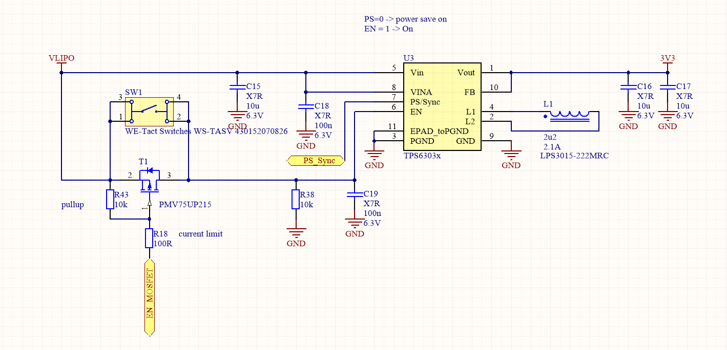
As you can see on the left side of the circuit above the self-sustaining circuit only consists of MOSFET T1, pull-up resistor R43 (and R18). R18 is not necessary but can protect the microcontroller pin connected to EN_MOSFET in the case of an overvoltage event.
First there is an error in noting the designators. In schematics, its T14 but you write it as T12 transistor.
“If you want to use this circuit in a 24V or even 48V environment Vgs needs to be limited. This is done by the zener diode D111. ”
Also, I don’t get why would you need a zener diode if PWR_IN is 24V. Since when the T14 turns ON and voltage will be 12V at the gate of T13 Mosfet. 24V(Source) – 12V(Gate) = 12V. Its still in max range of ±20V.
Could you please explain a bit more ?
You’re right, consider the zener diode as an additional mechanism of protection for T13. Depending on the power supply you’re hooked to (like in a automotive environment) or with simple ESD events it’s easy to exceed +/-20Vgs.